Engineering design is the foundation of every successful electronic device. A mistake at this stage is costly to fix later — in redesign, in delays, in a production run that doesn't perform as expected. That is why we approach the design phase thoroughly, without rushing and without shortcuts.
The process begins with a conversation. Together with the client we define what the device needs to do, under what conditions, with what power supply, which interfaces, and within what physical dimensions. Only once the requirements are clearly defined does the technical work begin.
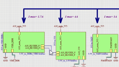
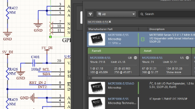
The first step is electrical schematic design — the logical blueprint that defines all components and their interconnections. This is the foundation on which everything else is built. We select components that are available on the market, that meet the project requirements, and that have a secure supply chain — because designing around a component that won't be available tomorrow is not a solution.
Once the schematic is finalised, PCB design begins — the physical layout of components and traces on the board. This is the phase where theory meets physical constraints: dimensions, heat management, electromagnetic compatibility, mechanical integration into the enclosure. A good PCB design is not only correct — it is robust, manufacturable, and suitable for series production.
At the end of the process the client receives complete technical documentation: the schematic, Gerber files, BOM list, and everything needed for production — whether with us or elsewhere.