PCB design is the phase where the abstraction of the schematic becomes physical reality. Every decision about component placement, signal routing and layer stackup has direct consequences on whether the device will work correctly — or not. Experience cannot be replaced by theory here.
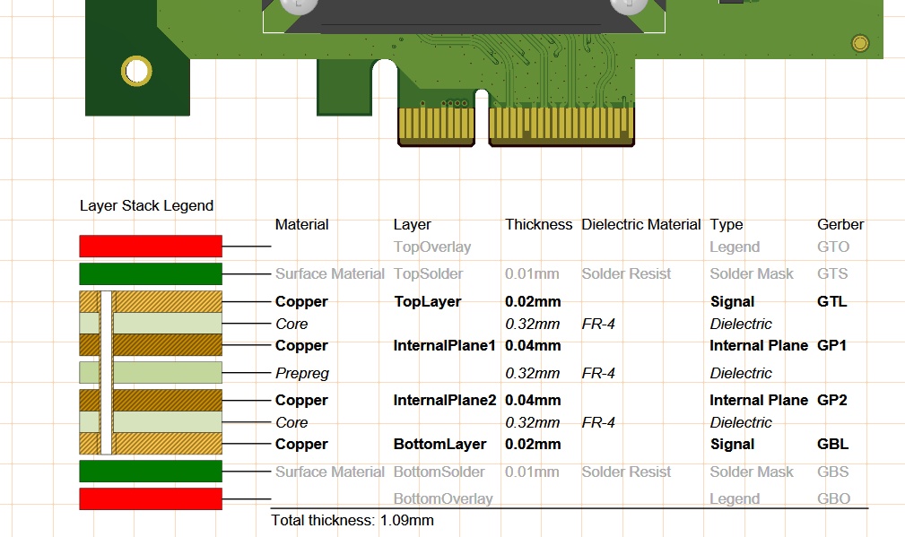
The process begins with importing the netlist from the schematic and defining the stackup. The number of layers, their purpose, dielectric thickness and copper weight — all of this is defined according to the project requirements and the capabilities of the chosen PCB manufacturer. For projects with controlled impedance or high-frequency signals, the stackup is not an aesthetic choice — it is an engineering specification.
Placement is done carefully and according to a clear signal flow logic. Critical components go first: voltage regulators close to the power input, decoupling capacitors as close as possible to the pins they serve, oscillators and crystals isolated from noise sources. Connectors are positioned according to the mechanical requirements of the enclosure. Only after the critical placement is locked does routing begin.
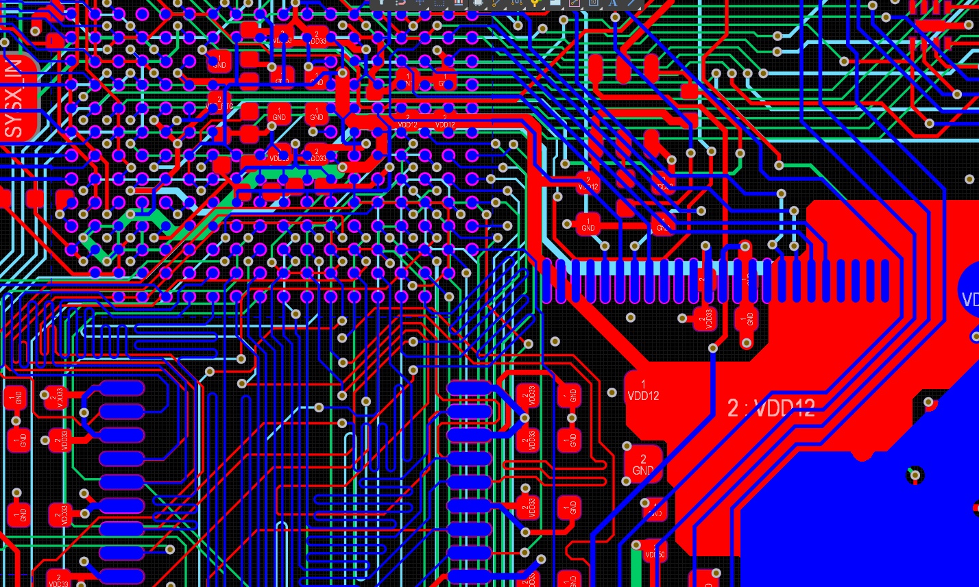
Routing is not simply connecting points with wires. Differential pairs are managed with controlled spacing and matched length. High-frequency signals get short, clean paths with a minimum number of vias. Analogue and digital signals are kept separate wherever possible. Return currents have clear paths — because whatever we do not define consciously, nature will define on its own, and rarely in our favour.
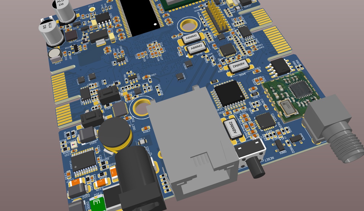
Particular attention goes to thermal management. Power components with significant dissipation are placed with access to airflow or with thermal vias to inner copper planes. Thermal pads beneath components such as LDOs, MOSFETs or power modules are routed according to the component manufacturer's guidelines — because poor thermal design in the first batch means overheating in the third.
Before finalisation, every design goes through DRC — Design Rule Check against rules aligned with the tolerances of the chosen PCB manufacturer. We verify clearances, minimum trace widths, via specifications, silk screen and everything that can cause problems in fabrication or assembly. Finally we generate complete fabrication documentation: Gerber files, drill files, assembly drawing and pick&place coordinate file for assembly.
If the client has their own PCB design that needs review or rework — that is equally welcome. We also carry out Design for Manufacturability reviews — checking whether the design is optimally adapted for pick&place assembly, which is particularly useful for clients who designed internally without experience in industrial assembly.