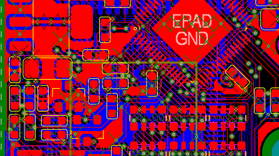
Once the schematic is complete and components selected, the project moves into the phase that will physically define the device — printed circuit board design. A PCB is more than a mechanical carrier for components; it is the substrate through which signals flow, through which heat is managed, which determines electromagnetic compatibility, and which ultimately must be manufacturable — in prototype and in series.
We design PCBs across the full spectrum of project complexity. Simple two-layer boards for power and control, through to multilayer boards with controlled impedance, high-frequency RF sections, BGA components and dense routing that demands experience and discipline. Every project is treated according to its actual requirements — without over-engineering where it is not needed, and without compromise where it is.
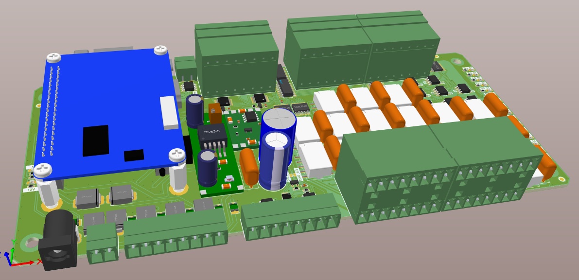
It is particularly important to us that every PCB design leaving our workshop is not only correct, but also manufacturable. This means tolerances are matched to the real capabilities of the fabrication house, component placement is adapted for automatic assembly on a pick&place line, and complete fabrication documentation accompanies the design from day one — not as an afterthought.
PCB design is available as part of our complete device development service, and also as a standalone service for clients who come with a finished schematic or who need a redesign of an existing board.